
AFM Substrates & Standards
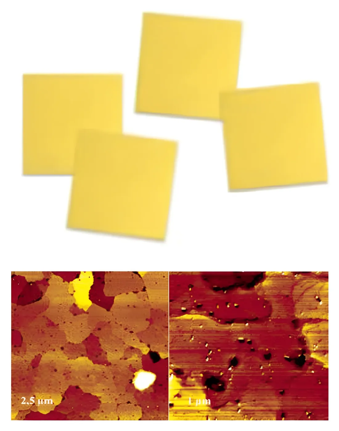
Gold Coated Silicon Wafer Substrates for AFM and STM
Conductive gold surfaces for nanoscale imaging, calibration and surface studies. Ask for pricing on wafers, gold thin film on mica and mica substrates.
- Conductive gold surfaces for AFM and STM imaging
- Also available: gold thin film on mica, small or large
- Made by Molecular Imaging, the AFM people since 1991
Built by the original Molecular Imaging AFM team, reunited after 2018.
Prefer to talk? Call 1-888-644-0389
Request substrate pricing
Tell us what you need. Our AFM team replies with pricing and options.
Why labs buy gold substrates from us
Conductive surface for electrical modes
Gold coated silicon and gold on mica suit STM, conductive AFM and electrochemical work.
Flat, well characterized surfaces
Gold thin film on mica gives a surface suited to calibration and roughness measurement.
Two formats of gold on mica
Choose the small format for routine samples or the large format for bigger scan areas.
Made by AFM people
The same team that built Molecular Imaging AFM systems makes and supports these substrates.
Full substrate and standards line
Add mica substrates, 500 nm gratings and step height standards in one order.
Real technical help
Ask our AFM specialists about mounting, holders and imaging in air or liquid.
Gold substrates and sample supports for AFM/STM
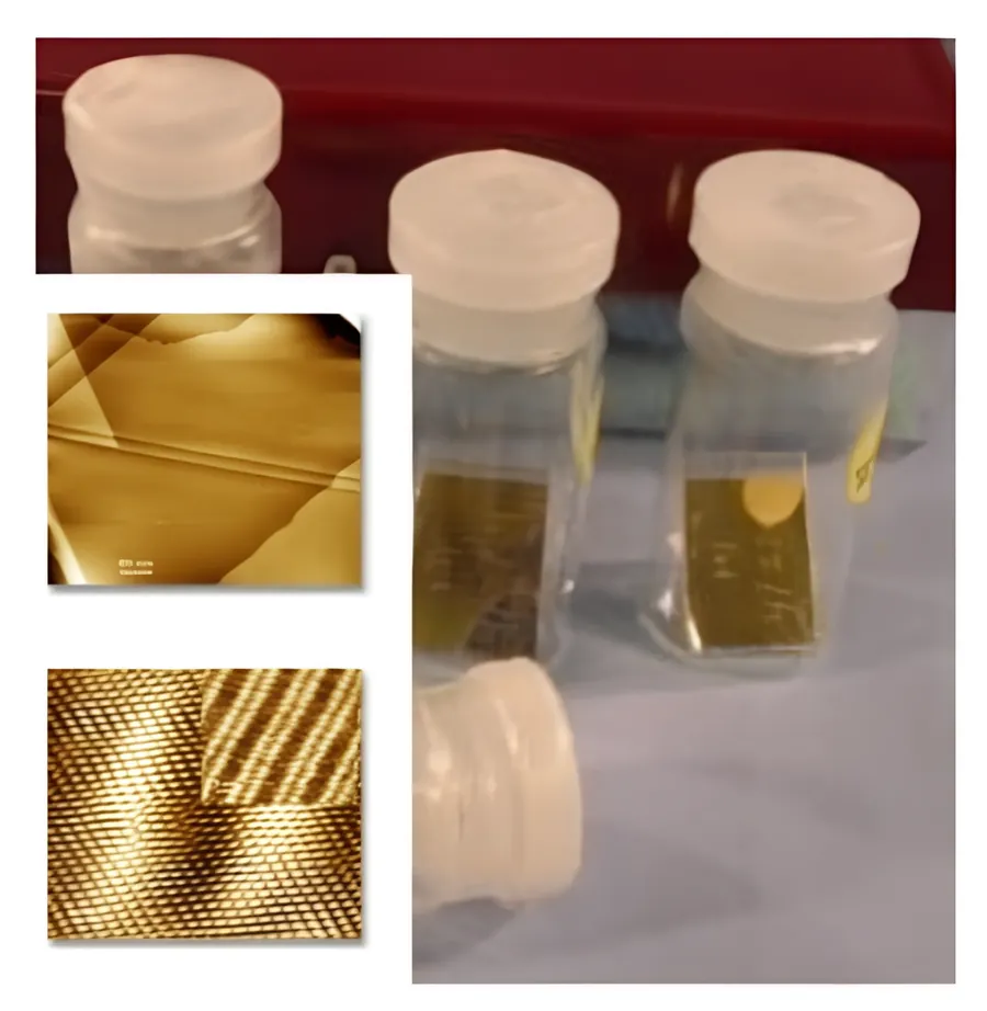
Molecular Imaging supplies gold coated silicon wafers and AU gold thin film on mica substrates for atomic force microscopy and scanning tunneling microscopy. Gold surfaces are used for AFM calibration, surface roughness measurement, thin film characterization and nanoscale material analysis.
We also make the holders and cells that go with them, so you can image the same substrate in air or fully in liquid. Tell us your sample size and imaging mode and we will confirm what fits.
- Gold coated silicon wafers for AFM substrate applications and nanoscale surface analysis
- AU gold thin film on mica substrate, small format, for AFM calibration and surface characterization
- AU gold thin film on mica substrate, large format, for roughness and thin film studies
- Mica substrate, 2 cm, atomically flat for sample preparation and high-resolution imaging
- Thin film sample holders for 22 mm x 22 mm substrates, cover slips, mica and HOPG
- One-inch and square cell holder formats, plus modular and custom holders
- Ambient and in-liquid imaging supported with our AFM liquid cells
- Calibration standards available too: 500 nm grating and step-height standards
What happens next
You send your request
Share the substrate type, format and quantity you need for your lab.
We review the fit
Our AFM team checks sizes, holders and imaging mode against your setup.
You get pricing
We reply with pricing and options so you can order with confidence.
Frequently asked questions
How much does a gold coated silicon wafer cost?
Pricing is available on request. Send your format and quantity and we will quote it. Prices are not published in our catalog.
Do you sell gold on mica as well as gold coated silicon?
Yes. We offer AU gold thin film on mica substrates in small and large formats, plus gold coated silicon wafers and 2 cm mica substrates.
Will these substrates work with my AFM?
Gold substrates are used for general AFM and STM work. We also supply thin film sample holders for 22 mm x 22 mm substrates, cover slips, mica and HOPG. Tell us your system and sample size and we will confirm the right holder.
Can I image these substrates in liquid?
Yes. Our thin film holders support ambient and in-liquid imaging, and we offer liquid cells including 1-inch, mini, PTFE and flow-through cells.
Do you also sell calibration standards?
Yes. We supply AFM calibration samples with a 500 nm periodic grating, step-height standards for Z-axis calibration, and N-type and P-type dopant standards.
Where do you ship from and who do you serve?
We are based at 30100 Telegraph Rd #337, Bingham Farms, MI. We serve the United States nationwide and market to the global research community.
Get pricing on gold coated silicon wafers
Tell us the substrate format and quantity your lab needs. Our AFM team will send pricing and suggest the right holders and standards to go with it.
- Conductive gold surfaces for AFM and STM imaging
- Also available: gold thin film on mica, small or large
- Made by Molecular Imaging, the AFM people since 1991
Prefer to talk? Call 1-888-644-0389